


SG-8018CB
- Brand: EPSON
- Size/Package: 5.0 x 3.2 x 1.1 mm
- Parameter: 0.67-170MHz
- Supply Voltage: 1.62-3.63V
- Output: CMOS
- Freq Tolerance: ±50ppm
- Operating Temp: -40℃~+105℃
- Package: 4P 5032
- Parameters
- Brand: EPSON
- Size/Package: 5.0 x 3.2 x 1.1 mm
- Parameter: 0.67-170MHz
- Supply Voltage: 1.62-3.63V
- Output: CMOS
- Freq Tolerance: ±50ppm
- Operating Temp: -40℃~+105℃
- Package: 4P 5032
Specifications
| Item | Symbol | Specifications | Conditions/Remarks | |||||||||||||
|---|---|---|---|---|---|---|---|---|---|---|---|---|---|---|---|---|
| Supply voltage | VCC | 1.80 V Typ. | 2.50 V Typ. | 3.30 V Typ. | ||||||||||||
| 1.62 to 1.98V | 1.98 to 2.20V | 2.20 to 2.80V | 2.70 to 3.63V | |||||||||||||
| Output frequency range | f0 | 0.67 MHz to 170 MHz | ||||||||||||||
| Storage temperature | T_stg | -40°C to +125°C | Storage as single product. | |||||||||||||
| Operating temperature | T_use | H: -40°C to +105°C | ||||||||||||||
| Frequency tolerance *1 | f_tol | J: ±50 × 10-6 | T_use= -40°C to +105°C | |||||||||||||
| Current consumption | ICC | 3.2mA Max. | 3.3mA Max. | 3.4mA Max. | 3.5mA Max. | T_use=+105°C | No load f0 = 20 MHz | |||||||||
| 2.7mA Typ. | 2.9mA Typ. | 3.0mA Typ. | T_use=+25°C | |||||||||||||
| 5.5mA Max. | 5.8mA Max. | 6.7mA Max. | 8.1mA Max. | T_use=+105°C | No load f0 = 170 MHz | |||||||||||
| 4.7mA Typ. | 5.7mA Typ. | 6.8mA Typ. | T_use=+25°C | |||||||||||||
| Output disable current | I_dis | 3.2mA Max. | 3.2mA Max. | 3.3mA Max. | 3.5mA Max. | OE=GND , f0 = 170 MHz | ||||||||||
| Standby current | I_std | 0.9μA Max. | 1.0μA Max. | 1.5μA Max. | 2.5μA Max. | T_use=+105°C | ST = GND | |||||||||
| 0.3μA Typ. | 0.4μA Typ. | 0.5μA Typ. | 1.1μA Typ. | T_use=+25°C | ||||||||||||
| Symmetry | SYM | 45% to 55% | 50% VCC Level | |||||||||||||
| Output voltage (DC characteristics) | VOH | 90% VCC Min. | [mA] | |||||||||||||
| tr / tf | VCC | A | B | C | D | |||||||||||
| Default (f0>40MHz) Fast | IOH | -2.5 | -3.5 | -4.0 | -5.0 | |||||||||||
| IOL | 2.5 | 3.5 | 4.0 | 5.0 | ||||||||||||
| Default (f0≦40MHz) | IOH | -1.5 | -2.0 | -2.5 | -3.0 | |||||||||||
| VOL | 10% VCC Max. | IOL | 1.5 | 2.0 | 2.5 | 3.0 | ||||||||||
| Slow | IOH | -1.0 | -1.5 | -2.0 | -2.5 | |||||||||||
| IOL | 1.0 | 1.5 | 2.0 | 2.5 | ||||||||||||
| A: 1.62 to 1.98 V , B: 1.98 to 2.20 V C: 2.20 to 2.80 V , D: 2.70 to 3.63 V | ||||||||||||||||
| Output load condition | L_CMOS | 15pF Max. | ||||||||||||||
| Input voltage | VIH | 70% VCC Min. | OE or ST | |||||||||||||
| VIL | 30% VCC Max. | |||||||||||||||
| Rise and Fall time | Default | tr / tf | 3.0 ns Max. | f0 > 40MHz | 20% VCC to 80% VCC L_CMOS=15pF | |||||||||||
| 6.0 ns Max. | f0 ≦ 40MHz | |||||||||||||||
| Fast | 3.0 ns Max. | f0=0.67to170MHz | ||||||||||||||
| Slow | 10.0 ns Max. | f0=0.67to20MHz | ||||||||||||||
| Disable Time | t_stp | 1 μs Max. | Measured from the time OE or ST pin crosses 30 % VCC | |||||||||||||
| Enable Time | t_sta | 1 μs Max. | Measured from the time OE pin crosses 70 % VCC | |||||||||||||
| Resume Time | t_res | 3 ms Max. | Measured from the time ST pin crosses 70 % VCC | |||||||||||||
| Start-up time | t_str | 3 ms Max. | Measured from the time VCC reaches its rated minimum value, 1.62 V | |||||||||||||
| Frequency aging | f_aging | This is included in frequency tolerance specification | +25°C, 10 years | |||||||||||||
*1 Frequency tolerance includes initial frequency tolerance, temperature variation, supply voltage variation, reflow drift, load drift and aging (+25°C, 10 years).
Pin description
| Pin | Name | I/O type | Function | |
| 1 | OE | Input | Output enable | High: Specified frequency output from OUT pin |
| Low: Out pin is low (weak pull down), only output driver is disabled. | ||||
| ST | Input | Standby | High: Specified frequency output from OUT pin | |
| Low: Out pin is low (weak pull down) | ||||
| Device goes to standby mode. Supply current reduces to the least as I_std. | ||||
| 2 | GND | Power | Ground | |
| 3 | OUT | Output | Clock output | |
| 4 | VCC | Power | Power supply | |
Product name
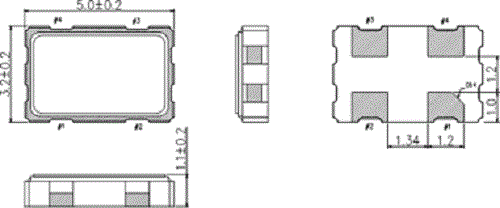
(Unit: mm)
To maintain stable operation, provide a 0.1µF by-pass capacitor at a location as near as possible to the power source terminal of the crystal product
(between VCC - GND).
Footprint
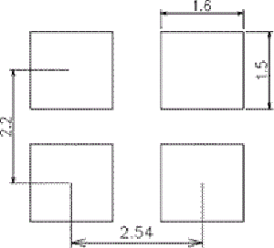
(Unit: mm)


 Copy product links
 Long by picture save/share
INQUIRY


Add Successfully
INQUIRY
Add Successfully

![]() Address:Rm805, Building B, Hongrongyuan, Mintang Rd, Shenzhen, China
Address:Rm805, Building B, Hongrongyuan, Mintang Rd, Shenzhen, China
Copyright By © YQM ELECTRONICS INTL LIMITED SITEMAP
Email: sales@yqmec.com

点击右上角
分享给朋友吧

