
NCES075P080LL: 750 V SiC MOSFET for High-Power Conversion
Time: 2026-11-13 07:29:54
NCES075P080LL: Design Checks for a 750 V SiC MOSFET
High-power converters usually run into the same two limits: heat that the enclosure cannot remove, and efficiency targets that a design almost — but not quite — reaches. Silicon carbide MOSFETs are often considered at that point. The NCES075P080LL is an NCE SiC MOSFET listed at 750 V, 37 A and 80 mΩ in a TOLL package. This article turns those verified parameters into a set of design checks rather than a performance claim.
1. Two Pressures in High-Power Conversion
The starting point is the loss budget, not the semiconductor material. Two recurring problems shape the selection:
- Thermal headroom. In high-current synchronous rectification and high-power output stages, conduction loss scales with I²·Rds(on). When the loss cannot be removed through the PCB and heatsink, engineers add copper, enlarge the heatsink or parallel devices — each of which adds cost and volume.
- Efficiency targets. In charging supplies, on-board DC-DC converters and SMPS designs, both full-load and light-load losses affect the efficiency figure. Switching-related losses become more prominent as frequency rises, so the device's switching behaviour and gate-drive conditions matter as much as its on-resistance.
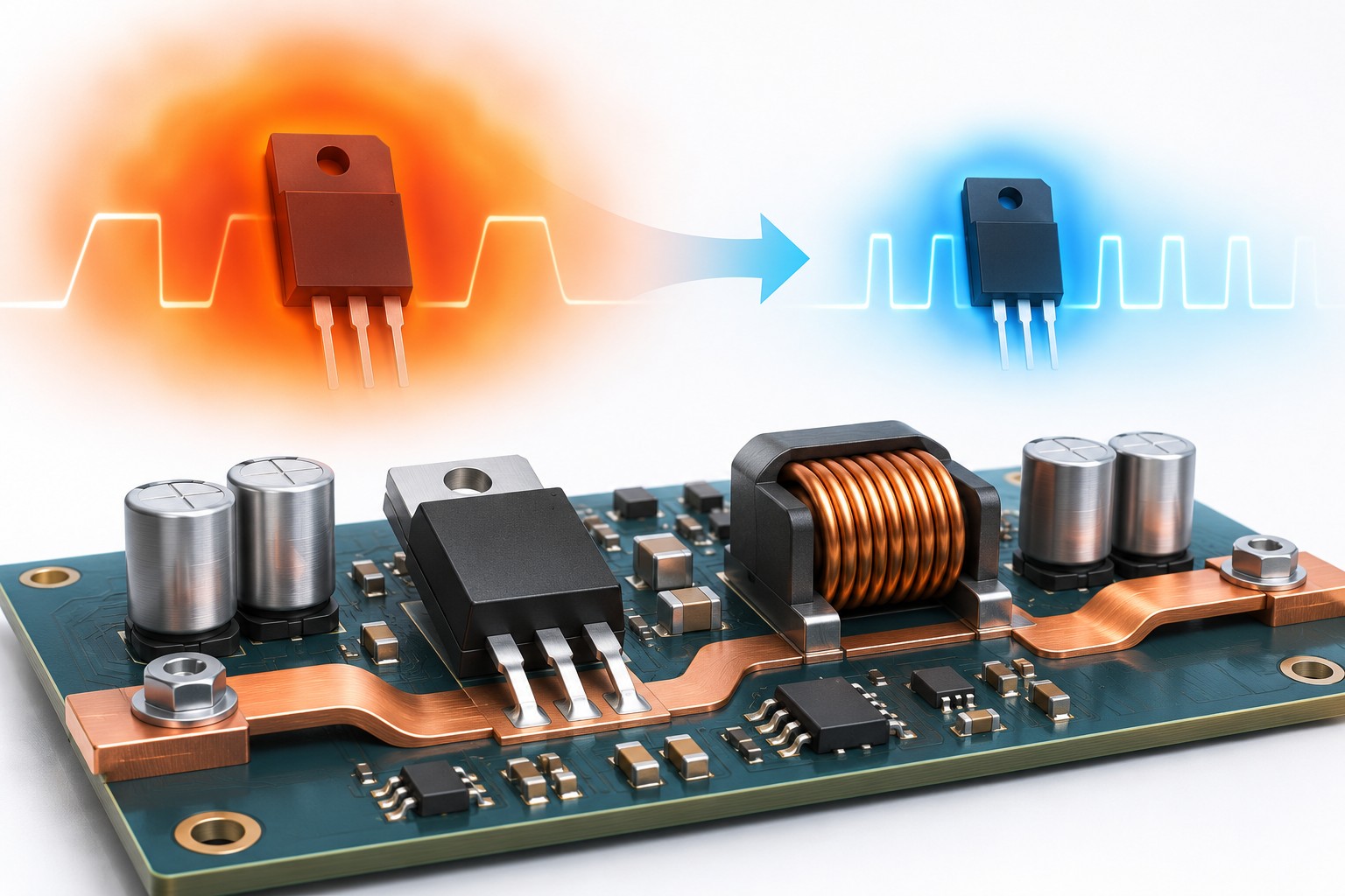
Figure 1: Conceptual view of switching and thermal behaviour in a power stage. Illustration only — no quantitative test result is implied.
2. What the Product Page Actually States
The following parameters are taken from the live product page. They are the only device figures used in this article; all other values and conditions must be confirmed in the manufacturer's datasheet before a design is released.
| Parameter | Value | Note |
|---|---|---|
| Part number | NCES075P080LL | NCE SiC MOSFET |
| Drain-source voltage | 750 V | As listed on the product page |
| Continuous drain current | 37 A | Confirm test conditions in the datasheet |
| On-state resistance | 80 mΩ | Typical value; confirm gate voltage and temperature |
| Package | TOLL | Surface-mount, compact footprint |
A note on scope: the product page does not publish switching energy, gate charge, SOA curves or thermal impedance in the fields quoted here. Those items belong to the datasheet, and any comparison with silicon super-junction or IGBT solutions requires measured data under identical conditions.
3. Conduction Loss and the Thermal Budget
For a resistive conduction path, P = I² × Rds(on). The 80 mΩ figure therefore needs to be read together with the actual current waveform, the operating temperature and the gate-drive voltage — Rds(on) is temperature dependent, and a room-temperature typical value is not a worst-case design number.
- Compute conduction loss at the real RMS current, not at the headline continuous-current figure.
- Check the Rds(on) versus temperature curve and the specified gate-source voltage before setting the thermal budget.
- Treat the TOLL package's thermal path — junction-to-case, board copper and airflow — as part of the design, since package choice and layout set how quickly heat leaves the die.
4. Switching Behaviour and Operating Frequency
SiC devices are frequently chosen when designers want to raise switching frequency and reduce the size of magnetics and capacitors. The device's switching characteristics matter here, but a frequency increase also changes gate-drive loss, layout parasitics and EMI behaviour. No efficiency gain should be assumed without a measurement at the intended bus voltage, current and temperature.
- Verify gate-charge and switching-energy figures in the datasheet at the intended drive voltage.
- Keep the gate loop short and review layout parasitics before increasing switching frequency.
- Validate EMI and thermal behaviour at full load after any frequency change.
5. Package, Layout and Reliability
The TOLL package is a compact surface-mount option. Its small footprint helps dense power boards, but it also concentrates the thermal path into the PCB, so copper area, via placement and assembly process deserve the same attention as the electrical parameters. For outdoor cabinets and industrial equipment, confirm the operating temperature range, humidity and reliability qualifications directly in the datasheet rather than relying on a general material property.
6. What to Verify Before Release
Use the product page to shortlist the device; use the datasheet and your own bench data to release it. The following checks are the minimum set for a high-power design:
- Absolute maximum ratings, including voltage derating and transient margin at the actual bus voltage.
- Rds(on) test conditions, temperature coefficient and continuous-current conditions.
- Switching energy, gate charge, SOA curves and thermal impedance.
- Gate-drive voltage, turn-on/turn-off resistance and layout parasitics.
- Thermal cycling, operating temperature range and reliability qualification for the target environment.
7. Where This Device Class Is Considered
The application list below reflects the design contexts in which a 750 V SiC MOSFET is typically evaluated. It is not a qualification statement for any specific end product.
- High-power AC-DC and DC-DC converter stages, including charging and server power supplies.
- On-board DC-DC converters where efficiency and power density compete for board area.
- Industrial SMPS and outdoor cabinets where thermal headroom is limited.
- High-frequency power stages where magnetics volume is a design constraint.
8. Frequently Asked Questions
Is 80 mΩ the worst-case on-resistance? It is the typical value listed on the product page. Check the datasheet for maximum values and for the gate voltage and junction temperature at which Rds(on) is specified.
Does a SiC MOSFET automatically improve efficiency? Not automatically. Conduction loss, switching loss, gate drive and layout all change together. Efficiency must be measured on the actual converter at the intended operating point.
What does the TOLL package change? It reduces board footprint and changes the thermal path: more heat leaves through the PCB and copper, so layout and assembly become part of the thermal design.
Where can I get the full electrical curves? Request the manufacturer's datasheet through the product page or contact our team for documentation and FAE review.
9. Samples, Datasheets and FAE Support
As an authorized NCE distributor, YQM can supply the NCES075P080LL together with datasheets, samples and FAE support for volume programmes. If you are evaluating a 750 V SiC stage, our team can help review the loss budget, gate-drive plan and thermal layout — contact us for documentation.
Request Datasheet, Samples & FAE Review
●750 V / 37 A / 80 mΩ
●TOLL surface-mount package
●Loss-budget review
●Datasheet & samples
NCES075P080LL: 750 V SiC MOSFET for High-Power Conversion
Time: 2026-11-13 07:29:54
NCES075P080LL: Design Checks for a 750 V SiC MOSFET
High-power converters usually run into the same two limits: heat that the enclosure cannot remove, and efficiency targets that a design almost — but not quite — reaches. Silicon carbide MOSFETs are often considered at that point. The NCES075P080LL is an NCE SiC MOSFET listed at 750 V, 37 A and 80 mΩ in a TOLL package. This article turns those verified parameters into a set of design checks rather than a performance claim.
1. Two Pressures in High-Power Conversion
The starting point is the loss budget, not the semiconductor material. Two recurring problems shape the selection:
- Thermal headroom. In high-current synchronous rectification and high-power output stages, conduction loss scales with I²·Rds(on). When the loss cannot be removed through the PCB and heatsink, engineers add copper, enlarge the heatsink or parallel devices — each of which adds cost and volume.
- Efficiency targets. In charging supplies, on-board DC-DC converters and SMPS designs, both full-load and light-load losses affect the efficiency figure. Switching-related losses become more prominent as frequency rises, so the device's switching behaviour and gate-drive conditions matter as much as its on-resistance.
Figure 1: Conceptual view of switching and thermal behaviour in a power stage. Illustration only — no quantitative test result is implied.
2. What the Product Page Actually States
The following parameters are taken from the live product page. They are the only device figures used in this article; all other values and conditions must be confirmed in the manufacturer's datasheet before a design is released.
| Parameter | Value | Note |
|---|---|---|
| Part number | NCES075P080LL | NCE SiC MOSFET |
| Drain-source voltage | 750 V | As listed on the product page |
| Continuous drain current | 37 A | Confirm test conditions in the datasheet |
| On-state resistance | 80 mΩ | Typical value; confirm gate voltage and temperature |
| Package | TOLL | Surface-mount, compact footprint |
A note on scope: the product page does not publish switching energy, gate charge, SOA curves or thermal impedance in the fields quoted here. Those items belong to the datasheet, and any comparison with silicon super-junction or IGBT solutions requires measured data under identical conditions.
3. Conduction Loss and the Thermal Budget
For a resistive conduction path, P = I² × Rds(on). The 80 mΩ figure therefore needs to be read together with the actual current waveform, the operating temperature and the gate-drive voltage — Rds(on) is temperature dependent, and a room-temperature typical value is not a worst-case design number.
- Compute conduction loss at the real RMS current, not at the headline continuous-current figure.
- Check the Rds(on) versus temperature curve and the specified gate-source voltage before setting the thermal budget.
- Treat the TOLL package's thermal path — junction-to-case, board copper and airflow — as part of the design, since package choice and layout set how quickly heat leaves the die.
4. Switching Behaviour and Operating Frequency
SiC devices are frequently chosen when designers want to raise switching frequency and reduce the size of magnetics and capacitors. The device's switching characteristics matter here, but a frequency increase also changes gate-drive loss, layout parasitics and EMI behaviour. No efficiency gain should be assumed without a measurement at the intended bus voltage, current and temperature.
- Verify gate-charge and switching-energy figures in the datasheet at the intended drive voltage.
- Keep the gate loop short and review layout parasitics before increasing switching frequency.
- Validate EMI and thermal behaviour at full load after any frequency change.
5. Package, Layout and Reliability
The TOLL package is a compact surface-mount option. Its small footprint helps dense power boards, but it also concentrates the thermal path into the PCB, so copper area, via placement and assembly process deserve the same attention as the electrical parameters. For outdoor cabinets and industrial equipment, confirm the operating temperature range, humidity and reliability qualifications directly in the datasheet rather than relying on a general material property.
6. What to Verify Before Release
Use the product page to shortlist the device; use the datasheet and your own bench data to release it. The following checks are the minimum set for a high-power design:
- Absolute maximum ratings, including voltage derating and transient margin at the actual bus voltage.
- Rds(on) test conditions, temperature coefficient and continuous-current conditions.
- Switching energy, gate charge, SOA curves and thermal impedance.
- Gate-drive voltage, turn-on/turn-off resistance and layout parasitics.
- Thermal cycling, operating temperature range and reliability qualification for the target environment.
7. Where This Device Class Is Considered
The application list below reflects the design contexts in which a 750 V SiC MOSFET is typically evaluated. It is not a qualification statement for any specific end product.
- High-power AC-DC and DC-DC converter stages, including charging and server power supplies.
- On-board DC-DC converters where efficiency and power density compete for board area.
- Industrial SMPS and outdoor cabinets where thermal headroom is limited.
- High-frequency power stages where magnetics volume is a design constraint.
8. Frequently Asked Questions
Is 80 mΩ the worst-case on-resistance? It is the typical value listed on the product page. Check the datasheet for maximum values and for the gate voltage and junction temperature at which Rds(on) is specified.
Does a SiC MOSFET automatically improve efficiency? Not automatically. Conduction loss, switching loss, gate drive and layout all change together. Efficiency must be measured on the actual converter at the intended operating point.
What does the TOLL package change? It reduces board footprint and changes the thermal path: more heat leaves through the PCB and copper, so layout and assembly become part of the thermal design.
Where can I get the full electrical curves? Request the manufacturer's datasheet through the product page or contact our team for documentation and FAE review.
9. Samples, Datasheets and FAE Support
As an authorized NCE distributor, YQM can supply the NCES075P080LL together with datasheets, samples and FAE support for volume programmes. If you are evaluating a 750 V SiC stage, our team can help review the loss budget, gate-drive plan and thermal layout — contact us for documentation.
Request Datasheet, Samples & FAE Review
●750 V / 37 A / 80 mΩ
●TOLL surface-mount package
●Loss-budget review
●Datasheet & samples
Other Articles
-

electronica 2026: Clock Tree & Power BOM Essentials
-
SiTime MEMS Timing for Industrial Automation: Precision Clocking for Smart Factories
-
NCES075P080LL: 750 V SiC MOSFET for High-Power Conversion
-
Epson RA4803SA RTC: Ultra-Low-Power Real-Time Clock for Portable & Industrial
-
Base Station Power MOSFET Selection: 8 NCE MOSFETs from 650V PFC to 48V Bus
-
Epson XV7021BB Gyroscope: QMEMS Angular Rate Sensor for UAV & Industrial AHRS
-
YQM FPC Connector Selection Guide: 0.5mm Pitch ZIF for Consumer & Wearable Devices
-
YSO510TP Drone TCXO: ±0.5 ppm from -40°C to +85°C
-
SiTime MEMS Timing for Aerospace & Defense: Precision PNT in Extreme Environments
-
SiTime PNT Timing Foundation: Why Precision Oscillators Define Modern Navigation


Copyright By © YQM ELECTRONICS INTL LIMITED SITEMAP
Email: sales@yqmec.com

点击右上角
分享给朋友吧


