
Base Station Power MOSFET Selection: 8 NCE MOSFETs from 650V PFC to 48V Bus
Time: 2026-11-10 11:38:28
Base-Station Power MOSFET Selection: From 650 V PFC to the 48 V Bus
5G and 5G-A roll-outs keep pushing telecom power supplies toward higher power density: the thermal budget tightens, the enclosure does not grow, and delivery schedules compress. MOSFET selection has to satisfy voltage class, conduction loss, package cooling and availability at the same time. This guide maps eight NCE devices onto one base-station power chain — starting with the 650 V NCE65NF050QD on the primary side — so each topology position has a concrete part number.
1. Start from the Power Chain, Not the Part Number
A typical base-station supply runs AC input → PFC boost → LLC resonant conversion → secondary rectification → 48 V DC bus → BBU/AAU loads. PFC and LLC work on a several-hundred-volt bus and need 600 V/650 V devices. On the 48 V output side, secondary synchronous rectification sits in the 150 V class and bus protection in the 80 V class; auxiliary supplies and load switches inside BBU/AAU units use 30 V parts. Rds(on) is the on-state resistance: lower values cut conduction loss, which matters most in high-current paths.
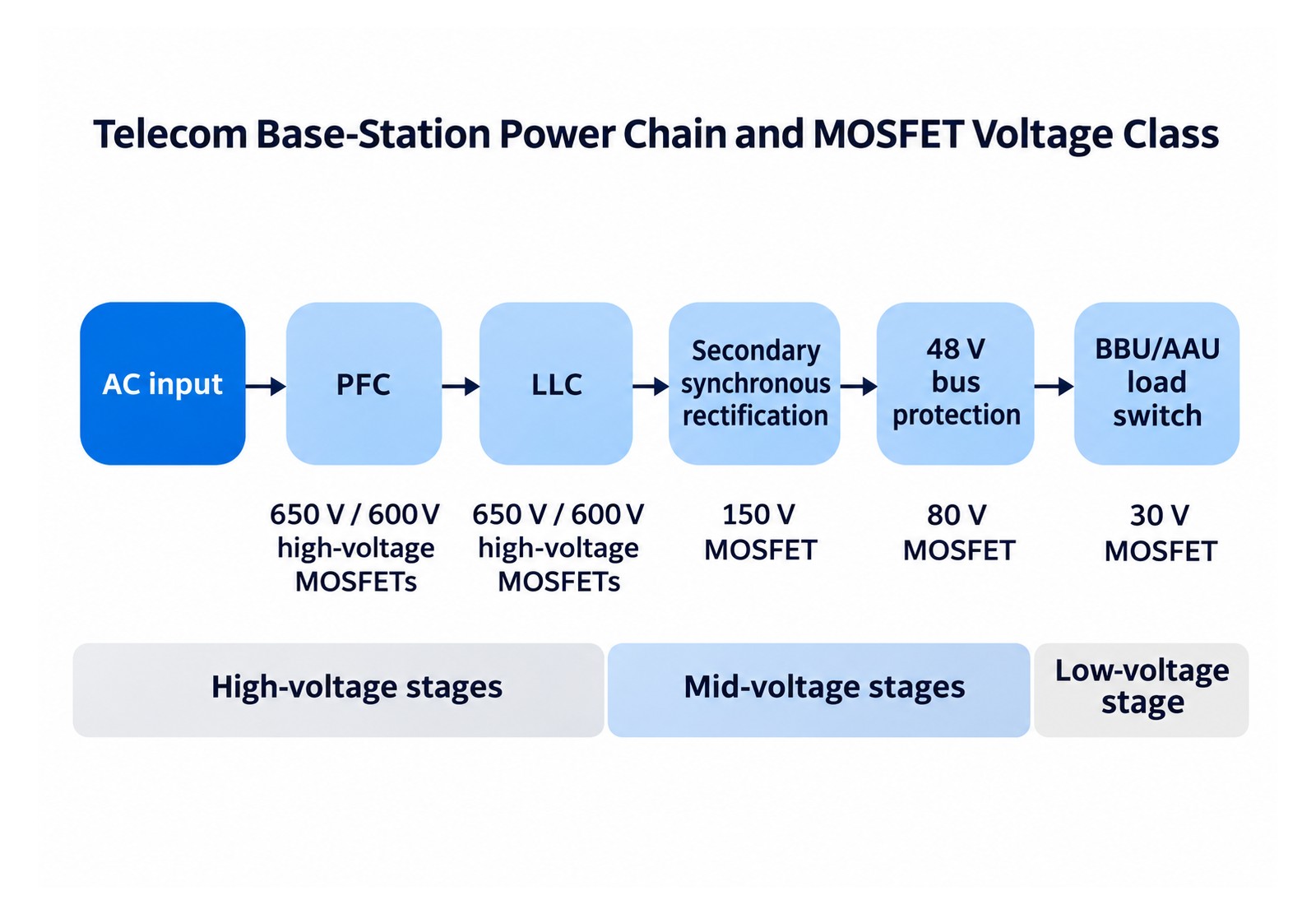
Figure 1: Voltage classes mapped onto the base-station power chain.
2. Primary Side: Four 650 V / 600 V Options
PFC boost raises the bus to roughly the 400 V level and LLC completes isolated conversion under soft switching, so both positions need high-voltage MOSFETs. NCE offers four Super-Junction options here, graded by on-state resistance and package. Low gate charge supports high-frequency, high-efficiency operation.
- NCE65NF050QD: 650 V / 56 A, 45 mΩ typical, QDPAK-22L top-side cooling — the high-power choice where full-load efficiency and thermal margin are tight.
- NCE65NF068T: 650 V / 45 A, 60 mΩ typical, TO-247-3L through-hole — the mainstream balance of cost and loss.
- NCE65NF099QD: 650 V / 36 A, 85 mΩ typical, QDPAK-22L — a compact mid-power option for smaller modules.
- NCE60NF055LL: 600 V / 51 A, 50 mΩ typical, TOLL — a surface-mount choice when PCB area is the constraint.
3. Secondary Synchronous Rectification: 150 V
On the 48 V output side, currents routinely exceed one hundred amps and conduction loss scales with I²R, so every milliohm matters. The 150 V class also leaves generous margin above a 48 V output and covers 110 V/120 V DC bus designs with the same topology.
- NCEP15T14D: 150 V / 140 A, 5.6 mΩ, TO-263-2L, Super Trench I, -55 to +175 °C.
- Drain-source voltage: 150 V, covering 48 V output rectification and 110 V/120 V DC bus use.
- Continuous drain current: 140 A at 25 °C; on-state resistance: 5.6 mΩ typical.
- Package: TO-263-2L with a wide operating temperature range.
4. 48 V Bus Protection: 80 V
The 48 V bus is the main artery of base-station power. OR-ing, hot-swap and battery charge/discharge protection all switch on this rail, where peak currents are high and switching is frequent. A low-voltage, high-current, low-Rds(on) device keeps voltage drop and heating under control.
- NCEP021NH80GU: 80 V / 244 A, 1.9 mΩ, DFN5×6-8L, Super Trench I.
- Drain-source voltage: 80 V, matched to 48 V bus switching and protection circuits.
- Continuous drain current: 244 A at 25 °C; on-state resistance: 1.9 mΩ typical.
- Package: DFN5×6-8L, -55 to +150 °C operating range.
5. Low-Voltage Auxiliary: 30 V N- and P-Channel
BBU/AAU auxiliary supplies, load switches and protection circuits sit in the 30 V class, with two clearly separated roles.
- N-channel NCEP3065QU: 30 V / 65 A, 1.3 mΩ at 10 V, DFN3.3×3.3-8L — the workhorse for auxiliary synchronous rectification and load switching where low loss and small footprint matter.
- P-channel NCE30P25S: -30 V / -25 A, 6.4 mΩ, SOP-8 — a common choice for reverse-polarity protection and high-side load switching, because a high-side P-channel switch needs no charge pump or bootstrap circuit.
6. Eight-Model Quick Reference
The table below collects the eight devices by voltage class. All values are typical figures from the manufacturer's datasheet; confirm test conditions and absolute maximum ratings before release.
| Voltage | Model | Id (25 °C) | Rds(on) typ. | Package | Chain position |
|---|---|---|---|---|---|
| 650 V | NCE65NF050QD | 56 A | 45 mΩ | QDPAK-22L | PFC / LLC primary |
| 650 V | NCE65NF068T | 45 A | 60 mΩ | TO-247-3L | PFC / LLC primary |
| 650 V | NCE65NF099QD | 36 A | 85 mΩ | QDPAK-22L | PFC / LLC primary |
| 600 V | NCE60NF055LL | 51 A | 50 mΩ | TOLL | PFC / LLC primary |
| 150 V | NCEP15T14D | 140 A | 5.6 mΩ | TO-263-2L | Secondary rectification |
| 80 V | NCEP021NH80GU | 244 A | 1.9 mΩ | DFN5×6-8L | 48 V bus protection |
| 30 V | NCEP3065QU | 65 A | 1.3 mΩ | DFN3.3×3.3-8L | Auxiliary / load switch |
| 30 V | NCE30P25S | -25 A | 6.4 mΩ | SOP-8 | Auxiliary / load switch |
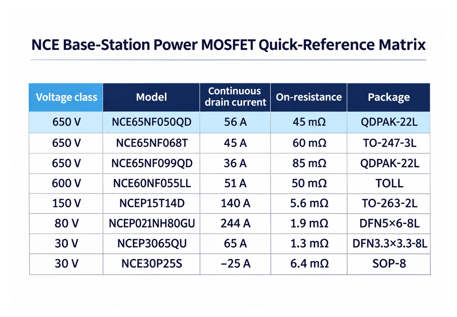
Figure 2: Quick-reference matrix of the eight NCE MOSFETs.
7. A Three-Step Selection Path
Working from the topology position back to device requirements is closer to real operating conditions than comparing single-device specifications in isolation.
- Fix the voltage class from the chain position. Once the position is fixed, the voltage class is essentially fixed too.
- Match Rds(on) and current to the loss budget. High-current paths justify the lowest on-resistance; cost-sensitive positions can use higher-resistance grades.
- Check package, cooling and availability. Through-hole, surface-mount and top-side-cooled packages imply different thermal designs and assembly processes; lock availability against the project schedule.
8. Frequently Asked Questions
Which parameter comes first? Voltage class and chain position. PFC/LLC primary stages use 600 V/650 V parts, secondary rectification on a 48 V output uses the 150 V class, bus protection uses 80 V, and BBU/AAU auxiliary circuits use 30 V.
How do the three 650 V options differ? By on-resistance and current grade: 45 mΩ/56 A targets high-power designs with tight efficiency limits, 60 mΩ/45 A is the mainstream balance, and 85 mΩ/36 A suits cost-sensitive mid-power designs.
P-channel or N-channel at 30 V? The N-channel NCEP3065QU offers lower on-resistance for high-current switching and synchronous rectification; the P-channel NCE30P25S simplifies high-side switching by removing the charge pump and bootstrap circuit.
TOLL or QDPAK? TOLL is a compact surface-mount package that saves PCB area; QDPAK provides top-side cooling for thermally constrained, high-density modules; TO-247 supports designs that favour serviceability and mature assembly processes.
9. Sourcing and FAE Support
As an authorized NCE distributor, YQM supplies these eight base-station power MOSFETs with datasheet, sample and FAE support for volume programmes. If you are still mapping a power chain, our team can review conduction loss, switching behaviour and package cooling with you — contact our team for documentation and selection review.
Request Datasheets, Samples & FAE Support
●650 V / 600 V primary stages
●150 V / 80 V low-Rds(on) devices
●30 V N- and P-channel options
●Topology-based selection review
Base Station Power MOSFET Selection: 8 NCE MOSFETs from 650V PFC to 48V Bus
Time: 2026-11-10 11:38:28
Base-Station Power MOSFET Selection: From 650 V PFC to the 48 V Bus
5G and 5G-A roll-outs keep pushing telecom power supplies toward higher power density: the thermal budget tightens, the enclosure does not grow, and delivery schedules compress. MOSFET selection has to satisfy voltage class, conduction loss, package cooling and availability at the same time. This guide maps eight NCE devices onto one base-station power chain — starting with the 650 V NCE65NF050QD on the primary side — so each topology position has a concrete part number.
1. Start from the Power Chain, Not the Part Number
A typical base-station supply runs AC input → PFC boost → LLC resonant conversion → secondary rectification → 48 V DC bus → BBU/AAU loads. PFC and LLC work on a several-hundred-volt bus and need 600 V/650 V devices. On the 48 V output side, secondary synchronous rectification sits in the 150 V class and bus protection in the 80 V class; auxiliary supplies and load switches inside BBU/AAU units use 30 V parts. Rds(on) is the on-state resistance: lower values cut conduction loss, which matters most in high-current paths.
Figure 1: Voltage classes mapped onto the base-station power chain.
2. Primary Side: Four 650 V / 600 V Options
PFC boost raises the bus to roughly the 400 V level and LLC completes isolated conversion under soft switching, so both positions need high-voltage MOSFETs. NCE offers four Super-Junction options here, graded by on-state resistance and package. Low gate charge supports high-frequency, high-efficiency operation.
- NCE65NF050QD: 650 V / 56 A, 45 mΩ typical, QDPAK-22L top-side cooling — the high-power choice where full-load efficiency and thermal margin are tight.
- NCE65NF068T: 650 V / 45 A, 60 mΩ typical, TO-247-3L through-hole — the mainstream balance of cost and loss.
- NCE65NF099QD: 650 V / 36 A, 85 mΩ typical, QDPAK-22L — a compact mid-power option for smaller modules.
- NCE60NF055LL: 600 V / 51 A, 50 mΩ typical, TOLL — a surface-mount choice when PCB area is the constraint.
3. Secondary Synchronous Rectification: 150 V
On the 48 V output side, currents routinely exceed one hundred amps and conduction loss scales with I²R, so every milliohm matters. The 150 V class also leaves generous margin above a 48 V output and covers 110 V/120 V DC bus designs with the same topology.
- NCEP15T14D: 150 V / 140 A, 5.6 mΩ, TO-263-2L, Super Trench I, -55 to +175 °C.
- Drain-source voltage: 150 V, covering 48 V output rectification and 110 V/120 V DC bus use.
- Continuous drain current: 140 A at 25 °C; on-state resistance: 5.6 mΩ typical.
- Package: TO-263-2L with a wide operating temperature range.
4. 48 V Bus Protection: 80 V
The 48 V bus is the main artery of base-station power. OR-ing, hot-swap and battery charge/discharge protection all switch on this rail, where peak currents are high and switching is frequent. A low-voltage, high-current, low-Rds(on) device keeps voltage drop and heating under control.
- NCEP021NH80GU: 80 V / 244 A, 1.9 mΩ, DFN5×6-8L, Super Trench I.
- Drain-source voltage: 80 V, matched to 48 V bus switching and protection circuits.
- Continuous drain current: 244 A at 25 °C; on-state resistance: 1.9 mΩ typical.
- Package: DFN5×6-8L, -55 to +150 °C operating range.
5. Low-Voltage Auxiliary: 30 V N- and P-Channel
BBU/AAU auxiliary supplies, load switches and protection circuits sit in the 30 V class, with two clearly separated roles.
- N-channel NCEP3065QU: 30 V / 65 A, 1.3 mΩ at 10 V, DFN3.3×3.3-8L — the workhorse for auxiliary synchronous rectification and load switching where low loss and small footprint matter.
- P-channel NCE30P25S: -30 V / -25 A, 6.4 mΩ, SOP-8 — a common choice for reverse-polarity protection and high-side load switching, because a high-side P-channel switch needs no charge pump or bootstrap circuit.
6. Eight-Model Quick Reference
The table below collects the eight devices by voltage class. All values are typical figures from the manufacturer's datasheet; confirm test conditions and absolute maximum ratings before release.
| Voltage | Model | Id (25 °C) | Rds(on) typ. | Package | Chain position |
|---|---|---|---|---|---|
| 650 V | NCE65NF050QD | 56 A | 45 mΩ | QDPAK-22L | PFC / LLC primary |
| 650 V | NCE65NF068T | 45 A | 60 mΩ | TO-247-3L | PFC / LLC primary |
| 650 V | NCE65NF099QD | 36 A | 85 mΩ | QDPAK-22L | PFC / LLC primary |
| 600 V | NCE60NF055LL | 51 A | 50 mΩ | TOLL | PFC / LLC primary |
| 150 V | NCEP15T14D | 140 A | 5.6 mΩ | TO-263-2L | Secondary rectification |
| 80 V | NCEP021NH80GU | 244 A | 1.9 mΩ | DFN5×6-8L | 48 V bus protection |
| 30 V | NCEP3065QU | 65 A | 1.3 mΩ | DFN3.3×3.3-8L | Auxiliary / load switch |
| 30 V | NCE30P25S | -25 A | 6.4 mΩ | SOP-8 | Auxiliary / load switch |
Figure 2: Quick-reference matrix of the eight NCE MOSFETs.
7. A Three-Step Selection Path
Working from the topology position back to device requirements is closer to real operating conditions than comparing single-device specifications in isolation.
- Fix the voltage class from the chain position. Once the position is fixed, the voltage class is essentially fixed too.
- Match Rds(on) and current to the loss budget. High-current paths justify the lowest on-resistance; cost-sensitive positions can use higher-resistance grades.
- Check package, cooling and availability. Through-hole, surface-mount and top-side-cooled packages imply different thermal designs and assembly processes; lock availability against the project schedule.
8. Frequently Asked Questions
Which parameter comes first? Voltage class and chain position. PFC/LLC primary stages use 600 V/650 V parts, secondary rectification on a 48 V output uses the 150 V class, bus protection uses 80 V, and BBU/AAU auxiliary circuits use 30 V.
How do the three 650 V options differ? By on-resistance and current grade: 45 mΩ/56 A targets high-power designs with tight efficiency limits, 60 mΩ/45 A is the mainstream balance, and 85 mΩ/36 A suits cost-sensitive mid-power designs.
P-channel or N-channel at 30 V? The N-channel NCEP3065QU offers lower on-resistance for high-current switching and synchronous rectification; the P-channel NCE30P25S simplifies high-side switching by removing the charge pump and bootstrap circuit.
TOLL or QDPAK? TOLL is a compact surface-mount package that saves PCB area; QDPAK provides top-side cooling for thermally constrained, high-density modules; TO-247 supports designs that favour serviceability and mature assembly processes.
9. Sourcing and FAE Support
As an authorized NCE distributor, YQM supplies these eight base-station power MOSFETs with datasheet, sample and FAE support for volume programmes. If you are still mapping a power chain, our team can review conduction loss, switching behaviour and package cooling with you — contact our team for documentation and selection review.
Request Datasheets, Samples & FAE Support
●650 V / 600 V primary stages
●150 V / 80 V low-Rds(on) devices
●30 V N- and P-channel options
●Topology-based selection review
Other Articles
-

electronica 2026: Clock Tree & Power BOM Essentials
-
Base Station Power MOSFET Selection: 8 NCE MOSFETs from 650V PFC to 48V Bus
-
Epson XV7021BB Gyroscope: QMEMS Angular Rate Sensor for UAV & Industrial AHRS
-
Epson RA4803SA RTC: Ultra-Low-Power Real-Time Clock for Portable & Industrial
-
YQM FPC Connector Selection Guide: 0.5mm Pitch ZIF for Consumer & Wearable Devices
-
YSO510TP Drone TCXO: ±0.5 ppm from -40°C to +85°C
-
SiTime MEMS Timing for Aerospace & Defense: Precision PNT in Extreme Environments
-
Sunlord WCX Ultra-Low-Voltage Molded Power Inductors for 800G/1.6T AI Optical Modules
-
SiTime PNT Timing Foundation: Why Precision Oscillators Define Modern Navigation
-
YQ8563: Drop-In Low-Power RTC Replacement for NXP PCF8563


Copyright By © YQM ELECTRONICS INTL LIMITED SITEMAP
Email: sales@yqmec.com

点击右上角
分享给朋友吧


