
Optical Module Clocking: Epson Oscillators for 400G to 1.6T
Time: 2026-11-17 10:59:57
Inside 400G–1.6T Optical Modules: Three Clock Roles, Three Epson Oscillators
AI data-center build-out has compressed three optical generations into a few product cycles: 400G is in volume deployment, 800G is ramping and 1.6T has entered sampling. As PAM4 SerDes moves from 56G to 112G and toward 200G per lane, the eye margin at the receiver narrows, and the phase jitter of the reference clock becomes a line item in the link budget instead of a datasheet afterthought.
Epson divides the problem by role rather than by speed alone. The SG2520VGN packs an LVDS SPXO into a 2520 package for compact 1.6T OSFP designs; the SG3225VAN covers 73.5–700 MHz in the established 3225 footprint for 400G/800G QSFP-DD line-ups; and the TG5032CFN adds ±0.1 ppm temperature compensation for SyncE and 1588 PTP. YQM ELECTRONICS supplies all three and reviews clock trees against the Epson portfolio.
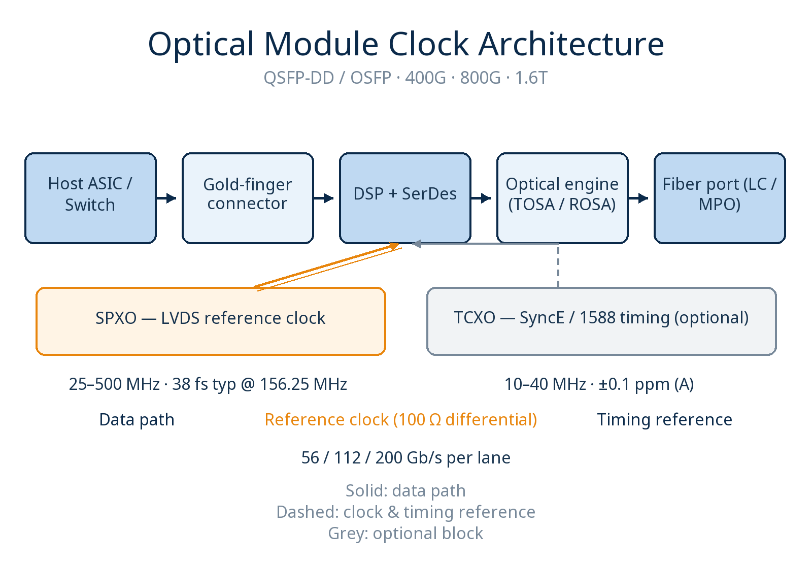
Figure 1. The LVDS oscillator drives the SerDes reference clock, while a TCXO supplies the synchronization reference where SyncE or 1588 PTP is required.
1. SPXO, TCXO and LVDS: What Each Term Decides
- SPXO. A simple packaged crystal oscillator combines a crystal and an oscillator die in one package. Differential versions drive SerDes reference inputs directly, so output standard, frequency range and phase jitter are the selection criteria rather than load capacitance.
- TCXO. A temperature-compensated crystal oscillator corrects the crystal's frequency drift with a compensation network. In optical transport it holds the synchronization time base; ±0.1 ppm class stability and aging dominate the choice.
- LVDS. Low-voltage differential signaling uses a 100 Ω differential pair with a small swing. Its common-mode rejection is what makes it the usual interface between a low-jitter oscillator and a high-speed SerDes.
2. Three Budgets That Decide the Clock Part
Optical-module clock selection is rarely a single-number decision. Three budgets pull in different directions, and each maps to a different device capability:
- Jitter budget. Compare RMS phase jitter only over the same integration band. The SG3225VAN is specified at 0.6 ps maximum over 12 kHz–20 MHz; the SG2520VGN is specified at 38 fs typical and 250 fs maximum at 156.25 MHz. Mixing integration bands turns a valid comparison into a misleading one.
- Board-space budget. A 2520 outline occupies roughly 5 mm² against roughly 8 mm² for a 3225 device, about 37% less. In an OSFP module the released area goes to the DSP, the optical subassembly and decoupling.
- Synchronization budget. SyncE and 1588 PTP are judged by holdover and time error across temperature and aging. This is TCXO territory, and it is measured in ppm rather than femtoseconds.
The three requirements do not compete for one device. A low-jitter SPXO cannot replace a TCXO in a synchronization path, and a TCXO is not chosen to minimize 156.25 MHz SerDes jitter. The practical clock tree often contains both.
3. SG2520VGN: A 2520-Package LVDS SPXO for 1.6T OSFP
The SG2520VGN is an LVDS SPXO in a 2.5 × 2.0 mm package. Its 25–500 MHz range covers the 156.25 MHz family used by high-speed SerDes and leaves headroom for higher reference frequencies. Typical RMS phase jitter is 38 fs at 156.25 MHz, with a 250 fs maximum, which keeps the clock contribution small inside a PAM4 link budget.
- Package: 2520 (2.5 × 2.0 mm) SMD
- Frequency range: 25–500 MHz
- Phase jitter: 38 fs typical @ 156.25 MHz; 250 fs maximum
- Frequency stability: ±25 ppm (D grade) / ±50 ppm (J grade)
- Supply voltage: 3.3 V / 2.5 V / 1.8 V options
- Operating temperature: -40 to +85 °C (G grade) / -40 to +105 °C (H grade)
For 1.6T OSFP layouts the headline is board area: about 5 mm² against about 8 mm² for a 3225 device, a reduction near 37%. The H grade extends operation to +105 °C for positions close to the DSP heat spreader, and the three supply options let the oscillator share a rail with the SerDes I/O instead of adding a regulator.
4. SG3225VAN: Wide-Band 3225 LVDS for 400G/800G QSFP-DD
The SG3225VAN is the wide-band member of the set: 73.5–700 MHz in a 3.2 × 2.5 mm LVDS oscillator, with 0.6 ps maximum phase jitter over the 12 kHz–20 MHz integration band. That frequency ceiling matters when a module uses a reference above the 500 MHz limit of the 2520 device, or when a mature 3225 layout should not be disturbed.
- Package: 3225 (3.2 × 2.5 mm) SMD
- Frequency range: 73.5–700 MHz
- Phase jitter: 0.6 ps maximum (12 kHz–20 MHz)
- Frequency stability: ±20 ppm (C grade) / ±30 ppm (E grade) / ±50 ppm (J grade)
- Supply voltage: 2.5–3.3 V
- Operating temperature: -20 to +70 °C (B grade) / -40 to +85 °C (G grade)
Because the 3225 footprint is already qualified on many 400G/800G QSFP-DD boards, this part is often the lower-risk choice for volume programs. The C grade's ±20 ppm suits thermally controlled designs; the G grade covers -40 to +85 °C for uncooled modules and industrial-temperature line cards.
5. TG5032CFN: A ±0.1 ppm TCXO for SyncE and 1588 PTP
The TG5032CFN changes function rather than merely frequency. It is a 5.0 × 3.2 mm CMOS TCXO covering 10–40 MHz, intended for synchronization references. Temperature stability is ±0.1 ppm in the A grade, ±0.25 ppm in the H grade and ±0.28 ppm in the B grade, with ±1.0 ppm initial deviation and ±0.5 ppm first-year aging (±3.0 ppm over 20 years).
- Type and output: TCXO, CMOS
- Package: 5032 (5.0 × 3.2 mm) SMD
- Frequency range: 10–40 MHz
- Temperature stability: ±0.1 ppm (A) / ±0.25 ppm (H) / ±0.28 ppm (B)
- Initial deviation and aging: ±1.0 ppm initial; ±0.5 ppm first year, ±3.0 ppm over 20 years
- Supply and temperature: 3.3 V (2.375–3.63 V), -40 to +85 °C
In a SyncE or 1588 line card the TCXO does not sit in the SerDes jitter path; it holds the network time base while the high-speed lanes run from a separate SPXO. The 3.3 V supply range and -40 to +85 °C rating match telecom line-card practice, and the two-device arrangement keeps each oscillator on the parameter that actually matters for its job.
6. Selection Matrix and Combined Specification Table
The matrix maps module class to oscillator role. The table reproduces the published numbers used in this article; confirm them against the current Epson datasheet before a design release.
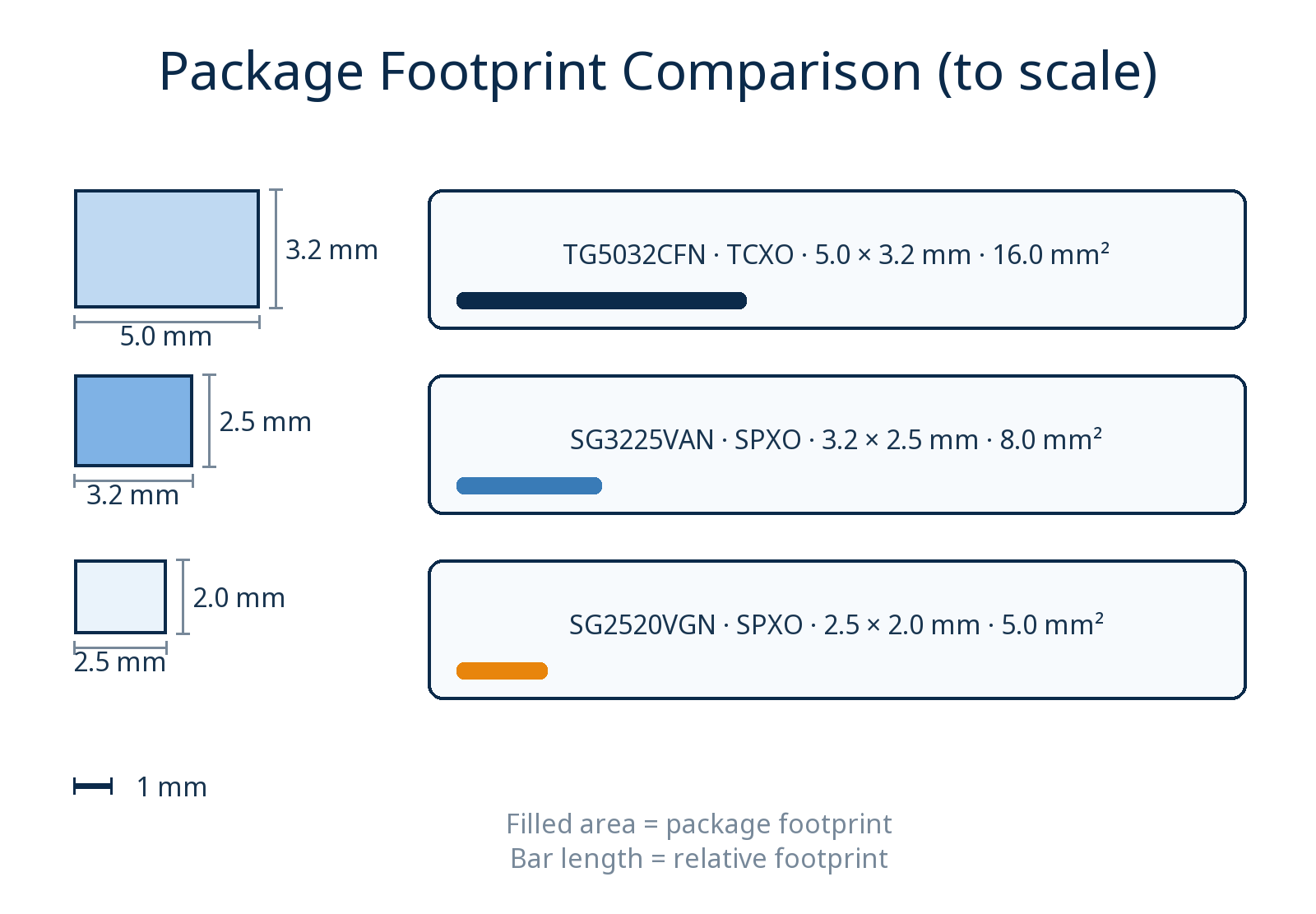
Figure 2. The three packages drawn to scale: 5032 for the TCXO, 3225 for the wide-band SPXO and 2520 for the compact 1.6T design.
| Model | Function / output | Package | Frequency range | Key clock metric | Supply | Temperature |
|---|---|---|---|---|---|---|
| SG2520VGN | SPXO, LVDS | 2520 (2.5 × 2.0 mm) | 25–500 MHz | 38 fs RMS typ @ 156.25 MHz; 250 fs max | 3.3 / 2.5 / 1.8 V | -40 to +85 °C (G) / -40 to +105 °C (H) |
| SG3225VAN | SPXO, LVDS | 3225 (3.2 × 2.5 mm) | 73.5–700 MHz | 0.6 ps max (12 kHz–20 MHz) | 2.5–3.3 V | -20 to +70 °C (B) / -40 to +85 °C (G) |
| TG5032CFN | TCXO, CMOS | 5032 (5.0 × 3.2 mm) | 10–40 MHz | ±0.1 ppm temperature stability (A) | 3.3 V (2.375–3.63 V) | -40 to +85 °C |
One variant is worth noting without changing the three-device structure: the SG3225CAN is a CMOS-output alternative in the same 3225 outline for interfaces that require a single-ended clock. It is an alternative, not a fourth main device in this comparison.
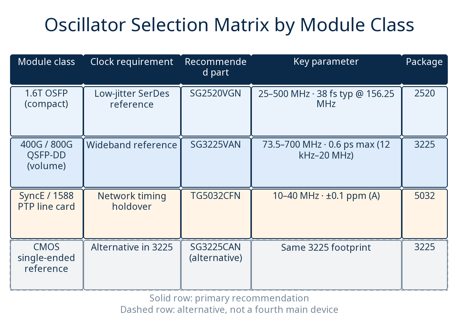
Figure 3. Selection by module class: compact 1.6T OSFP, volume 400G/800G QSFP-DD and synchronization-heavy line cards each point to a different role.
7. Five Checks Before You Freeze the Clock Tree
- Align the jitter integration band. Compare RMS phase jitter only over the same interval, for example 12 kHz–20 MHz, before comparing two oscillators.
- Route the differential pair as a pair. Keep the LVDS clock at 100 Ω differential impedance, with equal length and a short run to the SerDes reference pins.
- Decouple at the oscillator pin. Place the decoupling capacitor next to the supply pin; rail ripple modulates the output signal directly.
- Budget the footprint early. Decide between 2520 and 3225 while the PCB floor plan is still flexible, not after the optical subassembly is fixed.
- Separate synchronization from lane timing. Where SyncE or 1588 is required, plan a TCXO reference alongside the SPXO instead of over-specifying one device for both jobs.
8. Engineering FAQ
SPXO or TCXO? An SPXO has no temperature-compensation loop; it is selected for low jitter and frequency coverage. A TCXO adds compensation and reaches the ±0.1 ppm class for synchronization. High-speed lanes use the former, SyncE/1588 paths use the latter.
What does 38 fs mean in practice? A femtosecond is 10⁻¹⁵ s. At 156.25 MHz the period is 6.4 ns, so 38 fs is roughly six parts per million of one period — a small contribution to the jitter budget of a PAM4 SerDes.
Is the SG3225VAN LVDS or CMOS? It is an LVDS differential oscillator. For a CMOS output in the same 3225 footprint, evaluate the SG3225CAN as an alternative and confirm the interface level required by the SerDes or clock input.
Do I need both a TCXO and an SPXO? Not always. A module without synchronization needs only the SPXO. A module with SyncE or 1588 commonly uses a TCXO as the synchronization reference and a separate SPXO for the high-speed lanes.
Does the 2520 package sacrifice performance? The SG2520VGN is specified at 38 fs typical at 156.25 MHz with a 250 fs maximum. Check frequency, jitter, supply and temperature against the datasheet for the specific design; the smaller outline is not itself a performance penalty.
Can the TG5032CFN support 1588 PTP? Its ±0.1 ppm A-grade stability and ±0.5 ppm first-year aging provide a high-stability reference. End-to-end time error also depends on the holdover algorithm and network cascade, so include the oscillator in the system budget rather than evaluating it alone.
2520 or 3225 for a new 400G design? Use 2520 where board space is tight or the module class is 1.6T OSFP; use 3225 where the reference frequency exceeds 500 MHz or where an existing 3225 layout is already qualified.
9. Samples, Datasheets and Clock-Tree Review
As an authorized Epson distributor, YQM ELECTRONICS supports the SG2520VGN, SG3225VAN and TG5032CFN with samples, current datasheets and application review covering jitter-budget calculation, frequency-plan confirmation and alternative comparison. Browse the oscillators category, the differential oscillators range or the TCXO range, and contact our team with your module class, reference frequency and synchronization requirement.
Epson Optical-Module Clock Selection
●38 fs typ @ 156.25 MHz
●2520 / 3225 / 5032 packages
●±0.1 ppm TCXO for SyncE / 1588
●Samples, datasheets, FAE review
Optical Module Clocking: Epson Oscillators for 400G to 1.6T
Time: 2026-11-17 10:59:57
Inside 400G–1.6T Optical Modules: Three Clock Roles, Three Epson Oscillators
AI data-center build-out has compressed three optical generations into a few product cycles: 400G is in volume deployment, 800G is ramping and 1.6T has entered sampling. As PAM4 SerDes moves from 56G to 112G and toward 200G per lane, the eye margin at the receiver narrows, and the phase jitter of the reference clock becomes a line item in the link budget instead of a datasheet afterthought.
Epson divides the problem by role rather than by speed alone. The SG2520VGN packs an LVDS SPXO into a 2520 package for compact 1.6T OSFP designs; the SG3225VAN covers 73.5–700 MHz in the established 3225 footprint for 400G/800G QSFP-DD line-ups; and the TG5032CFN adds ±0.1 ppm temperature compensation for SyncE and 1588 PTP. YQM ELECTRONICS supplies all three and reviews clock trees against the Epson portfolio.
Figure 1. The LVDS oscillator drives the SerDes reference clock, while a TCXO supplies the synchronization reference where SyncE or 1588 PTP is required.
1. SPXO, TCXO and LVDS: What Each Term Decides
- SPXO. A simple packaged crystal oscillator combines a crystal and an oscillator die in one package. Differential versions drive SerDes reference inputs directly, so output standard, frequency range and phase jitter are the selection criteria rather than load capacitance.
- TCXO. A temperature-compensated crystal oscillator corrects the crystal's frequency drift with a compensation network. In optical transport it holds the synchronization time base; ±0.1 ppm class stability and aging dominate the choice.
- LVDS. Low-voltage differential signaling uses a 100 Ω differential pair with a small swing. Its common-mode rejection is what makes it the usual interface between a low-jitter oscillator and a high-speed SerDes.
2. Three Budgets That Decide the Clock Part
Optical-module clock selection is rarely a single-number decision. Three budgets pull in different directions, and each maps to a different device capability:
- Jitter budget. Compare RMS phase jitter only over the same integration band. The SG3225VAN is specified at 0.6 ps maximum over 12 kHz–20 MHz; the SG2520VGN is specified at 38 fs typical and 250 fs maximum at 156.25 MHz. Mixing integration bands turns a valid comparison into a misleading one.
- Board-space budget. A 2520 outline occupies roughly 5 mm² against roughly 8 mm² for a 3225 device, about 37% less. In an OSFP module the released area goes to the DSP, the optical subassembly and decoupling.
- Synchronization budget. SyncE and 1588 PTP are judged by holdover and time error across temperature and aging. This is TCXO territory, and it is measured in ppm rather than femtoseconds.
The three requirements do not compete for one device. A low-jitter SPXO cannot replace a TCXO in a synchronization path, and a TCXO is not chosen to minimize 156.25 MHz SerDes jitter. The practical clock tree often contains both.
3. SG2520VGN: A 2520-Package LVDS SPXO for 1.6T OSFP
The SG2520VGN is an LVDS SPXO in a 2.5 × 2.0 mm package. Its 25–500 MHz range covers the 156.25 MHz family used by high-speed SerDes and leaves headroom for higher reference frequencies. Typical RMS phase jitter is 38 fs at 156.25 MHz, with a 250 fs maximum, which keeps the clock contribution small inside a PAM4 link budget.
- Package: 2520 (2.5 × 2.0 mm) SMD
- Frequency range: 25–500 MHz
- Phase jitter: 38 fs typical @ 156.25 MHz; 250 fs maximum
- Frequency stability: ±25 ppm (D grade) / ±50 ppm (J grade)
- Supply voltage: 3.3 V / 2.5 V / 1.8 V options
- Operating temperature: -40 to +85 °C (G grade) / -40 to +105 °C (H grade)
For 1.6T OSFP layouts the headline is board area: about 5 mm² against about 8 mm² for a 3225 device, a reduction near 37%. The H grade extends operation to +105 °C for positions close to the DSP heat spreader, and the three supply options let the oscillator share a rail with the SerDes I/O instead of adding a regulator.
4. SG3225VAN: Wide-Band 3225 LVDS for 400G/800G QSFP-DD
The SG3225VAN is the wide-band member of the set: 73.5–700 MHz in a 3.2 × 2.5 mm LVDS oscillator, with 0.6 ps maximum phase jitter over the 12 kHz–20 MHz integration band. That frequency ceiling matters when a module uses a reference above the 500 MHz limit of the 2520 device, or when a mature 3225 layout should not be disturbed.
- Package: 3225 (3.2 × 2.5 mm) SMD
- Frequency range: 73.5–700 MHz
- Phase jitter: 0.6 ps maximum (12 kHz–20 MHz)
- Frequency stability: ±20 ppm (C grade) / ±30 ppm (E grade) / ±50 ppm (J grade)
- Supply voltage: 2.5–3.3 V
- Operating temperature: -20 to +70 °C (B grade) / -40 to +85 °C (G grade)
Because the 3225 footprint is already qualified on many 400G/800G QSFP-DD boards, this part is often the lower-risk choice for volume programs. The C grade's ±20 ppm suits thermally controlled designs; the G grade covers -40 to +85 °C for uncooled modules and industrial-temperature line cards.
5. TG5032CFN: A ±0.1 ppm TCXO for SyncE and 1588 PTP
The TG5032CFN changes function rather than merely frequency. It is a 5.0 × 3.2 mm CMOS TCXO covering 10–40 MHz, intended for synchronization references. Temperature stability is ±0.1 ppm in the A grade, ±0.25 ppm in the H grade and ±0.28 ppm in the B grade, with ±1.0 ppm initial deviation and ±0.5 ppm first-year aging (±3.0 ppm over 20 years).
- Type and output: TCXO, CMOS
- Package: 5032 (5.0 × 3.2 mm) SMD
- Frequency range: 10–40 MHz
- Temperature stability: ±0.1 ppm (A) / ±0.25 ppm (H) / ±0.28 ppm (B)
- Initial deviation and aging: ±1.0 ppm initial; ±0.5 ppm first year, ±3.0 ppm over 20 years
- Supply and temperature: 3.3 V (2.375–3.63 V), -40 to +85 °C
In a SyncE or 1588 line card the TCXO does not sit in the SerDes jitter path; it holds the network time base while the high-speed lanes run from a separate SPXO. The 3.3 V supply range and -40 to +85 °C rating match telecom line-card practice, and the two-device arrangement keeps each oscillator on the parameter that actually matters for its job.
6. Selection Matrix and Combined Specification Table
The matrix maps module class to oscillator role. The table reproduces the published numbers used in this article; confirm them against the current Epson datasheet before a design release.
Figure 2. The three packages drawn to scale: 5032 for the TCXO, 3225 for the wide-band SPXO and 2520 for the compact 1.6T design.
| Model | Function / output | Package | Frequency range | Key clock metric | Supply | Temperature |
|---|---|---|---|---|---|---|
| SG2520VGN | SPXO, LVDS | 2520 (2.5 × 2.0 mm) | 25–500 MHz | 38 fs RMS typ @ 156.25 MHz; 250 fs max | 3.3 / 2.5 / 1.8 V | -40 to +85 °C (G) / -40 to +105 °C (H) |
| SG3225VAN | SPXO, LVDS | 3225 (3.2 × 2.5 mm) | 73.5–700 MHz | 0.6 ps max (12 kHz–20 MHz) | 2.5–3.3 V | -20 to +70 °C (B) / -40 to +85 °C (G) |
| TG5032CFN | TCXO, CMOS | 5032 (5.0 × 3.2 mm) | 10–40 MHz | ±0.1 ppm temperature stability (A) | 3.3 V (2.375–3.63 V) | -40 to +85 °C |
One variant is worth noting without changing the three-device structure: the SG3225CAN is a CMOS-output alternative in the same 3225 outline for interfaces that require a single-ended clock. It is an alternative, not a fourth main device in this comparison.
Figure 3. Selection by module class: compact 1.6T OSFP, volume 400G/800G QSFP-DD and synchronization-heavy line cards each point to a different role.
7. Five Checks Before You Freeze the Clock Tree
- Align the jitter integration band. Compare RMS phase jitter only over the same interval, for example 12 kHz–20 MHz, before comparing two oscillators.
- Route the differential pair as a pair. Keep the LVDS clock at 100 Ω differential impedance, with equal length and a short run to the SerDes reference pins.
- Decouple at the oscillator pin. Place the decoupling capacitor next to the supply pin; rail ripple modulates the output signal directly.
- Budget the footprint early. Decide between 2520 and 3225 while the PCB floor plan is still flexible, not after the optical subassembly is fixed.
- Separate synchronization from lane timing. Where SyncE or 1588 is required, plan a TCXO reference alongside the SPXO instead of over-specifying one device for both jobs.
8. Engineering FAQ
SPXO or TCXO? An SPXO has no temperature-compensation loop; it is selected for low jitter and frequency coverage. A TCXO adds compensation and reaches the ±0.1 ppm class for synchronization. High-speed lanes use the former, SyncE/1588 paths use the latter.
What does 38 fs mean in practice? A femtosecond is 10⁻¹⁵ s. At 156.25 MHz the period is 6.4 ns, so 38 fs is roughly six parts per million of one period — a small contribution to the jitter budget of a PAM4 SerDes.
Is the SG3225VAN LVDS or CMOS? It is an LVDS differential oscillator. For a CMOS output in the same 3225 footprint, evaluate the SG3225CAN as an alternative and confirm the interface level required by the SerDes or clock input.
Do I need both a TCXO and an SPXO? Not always. A module without synchronization needs only the SPXO. A module with SyncE or 1588 commonly uses a TCXO as the synchronization reference and a separate SPXO for the high-speed lanes.
Does the 2520 package sacrifice performance? The SG2520VGN is specified at 38 fs typical at 156.25 MHz with a 250 fs maximum. Check frequency, jitter, supply and temperature against the datasheet for the specific design; the smaller outline is not itself a performance penalty.
Can the TG5032CFN support 1588 PTP? Its ±0.1 ppm A-grade stability and ±0.5 ppm first-year aging provide a high-stability reference. End-to-end time error also depends on the holdover algorithm and network cascade, so include the oscillator in the system budget rather than evaluating it alone.
2520 or 3225 for a new 400G design? Use 2520 where board space is tight or the module class is 1.6T OSFP; use 3225 where the reference frequency exceeds 500 MHz or where an existing 3225 layout is already qualified.
9. Samples, Datasheets and Clock-Tree Review
As an authorized Epson distributor, YQM ELECTRONICS supports the SG2520VGN, SG3225VAN and TG5032CFN with samples, current datasheets and application review covering jitter-budget calculation, frequency-plan confirmation and alternative comparison. Browse the oscillators category, the differential oscillators range or the TCXO range, and contact our team with your module class, reference frequency and synchronization requirement.
Epson Optical-Module Clock Selection
●38 fs typ @ 156.25 MHz
●2520 / 3225 / 5032 packages
●±0.1 ppm TCXO for SyncE / 1588
●Samples, datasheets, FAE review
Other Articles
-

Optical Module Clocking: Epson Oscillators for 400G to 1.6T
-
RX-8581SA End-of-Life: Migration Guide to Next-Gen RTC Alternatives
-
YQM FPC Connector Selection Guide: 0.3mm & 0.5mm Pitch for Consumer & Wearable Devices
-
Epson RA4803SA RTC: Ultra-Low-Power Real-Time Clock for Portable & Industrial
-
NCES075P080LL: 750 V SiC MOSFET for High-Power Conversion
-
SiTime MEMS Timing for Industrial Automation: Precision Clocking for Smart Factories
-
electronica 2026: Clock Tree & Power BOM Essentials
-
SiTime PNT Timing Foundation: Why Precision Oscillators Define Modern Navigation
-
Epson XV7021BB Gyroscope: QMEMS Angular Rate Sensor for UAV & Industrial AHRS
-
YSO510TP Drone TCXO: ±0.5 ppm from -40°C to +85°C


Copyright By © YQM ELECTRONICS INTL LIMITED SITEMAP
Email: sales@yqmec.com

点击右上角
分享给朋友吧


